We're hiring! Take the next step in your career with us.

Smarter Contamination Analysis

Helping you to increase chip production yields and reduce waste

Going further than ever before

Semiconductors today are increasingly sensitive to the smallest contaminations, which results in significant waste in the manufacturing process. 

As a result, billions of dollars are lost every year due to ineffective contamination control methods during the manufacturing process of semiconductors.

At UNISERS, we have developed a radically new technology to detect and characterize the smallest particles on any type of wafer. 

We’re proud to be at the forefront of change and innovation for this sector.

Universal Contamination Analysis

Innovative signal enhancement

UNISERS utilizes a one-of-a-kind vacuum-based plasma coating technology, designed to enhance the detection of contaminants on various surfaces, such as silicon wafers.

This innovative coating causes impurities to shine brightly, allowing our state-of-the-art optical scanner to easily identify and locate them for a cleaner, more efficient production process.

We're Hiring!

At UNISERS you would be working with cutting edge technologies and be solving some of the most challenging problems facing the semiconductor industry today. 

We’re a startup with big ambitions and even bigger plans, but we need talented people like you to bring those plans to life. 

Find out about the latest available roles on our Jobs page.

Why UNISERS?

Using our solution, you are able to find the source of contamination faster resulting in a massive cost and time savings compared to existing contamination analyzing solutions.

Our technology enables manufacturers to identify contaminations earlier in the process and in greater detail.

We are able to detect any nanoparticles down to 8nm. Our optical technology enables high detection speeds of any kind of contamination.

At UNISERS we develop all our own products and own the (IP) for all our solutions. 

With our ability to determine the size and type of particles using SEPS, whilst recording the molecular fingerprint from individual nanoparticles with our SERS technique is truly unique.

UNISERS is backed by trusted industry investors.

Our investors Intel Capital, M Ventures, Swisscom Ventures and RSBG Ventures are also actively supporting the company’s development.

Sustainability is an important aspect of our business which we take seriously. 

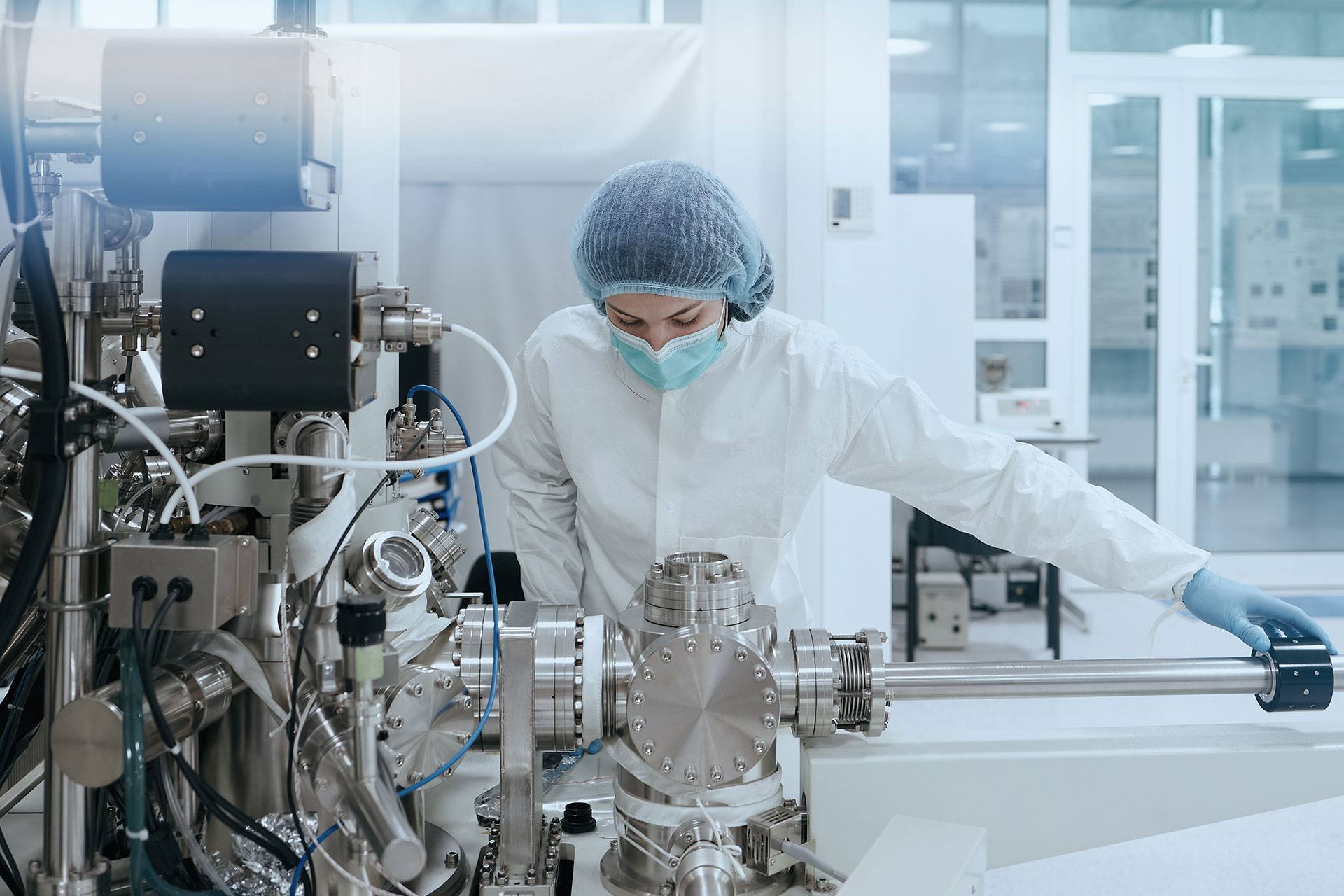
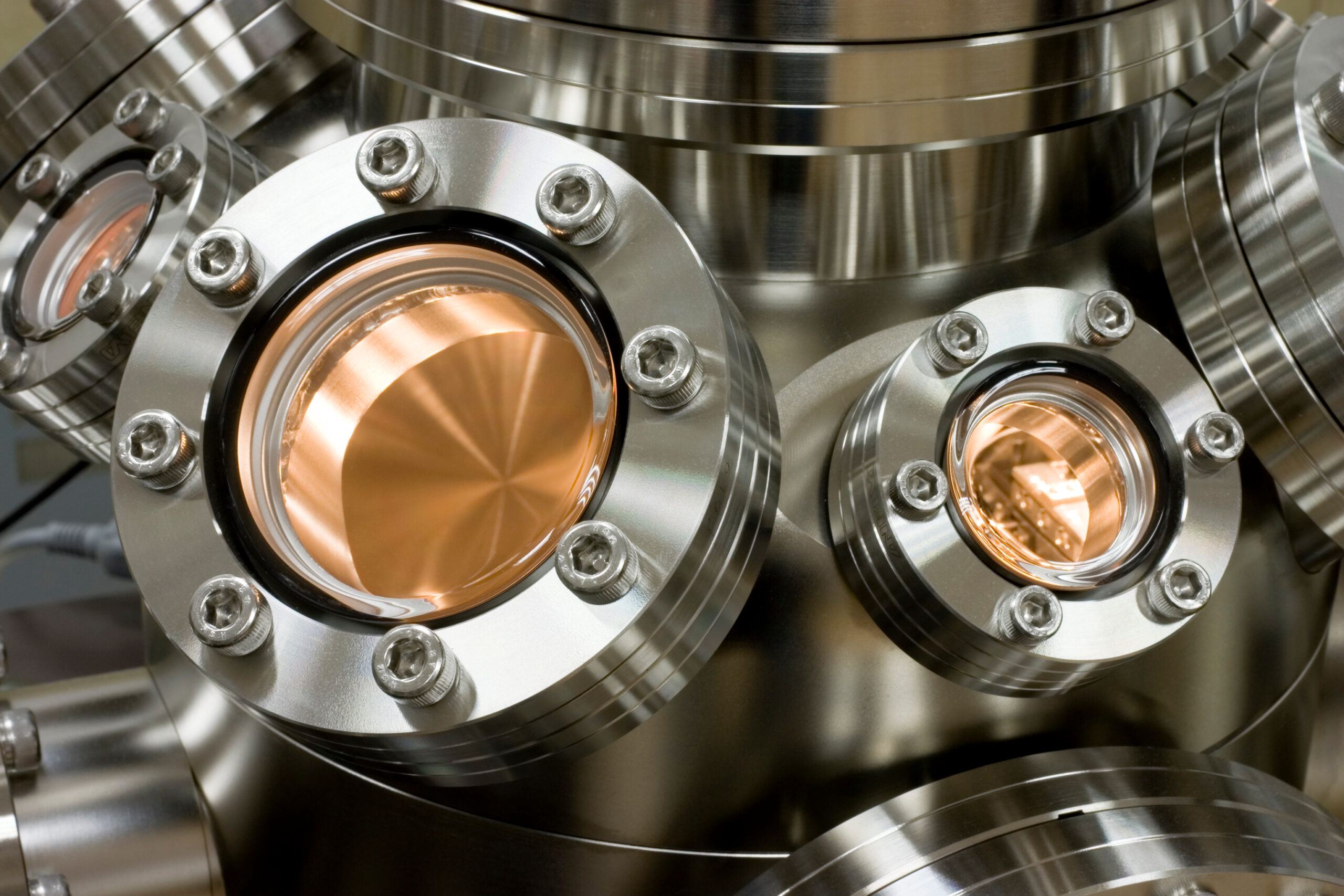
We are helping semiconductor manufacturers to reduce the amount of wasted chips (often more than 50%) which has the benefit of reducing waste and CO2 emissions.

Even a 1% improvement in semiconductor yield can save the industry 10 billions of liters of water, 500,000 tons of fossil fuels and 20,000 tons of gaseous emissions.

We're Award Winning