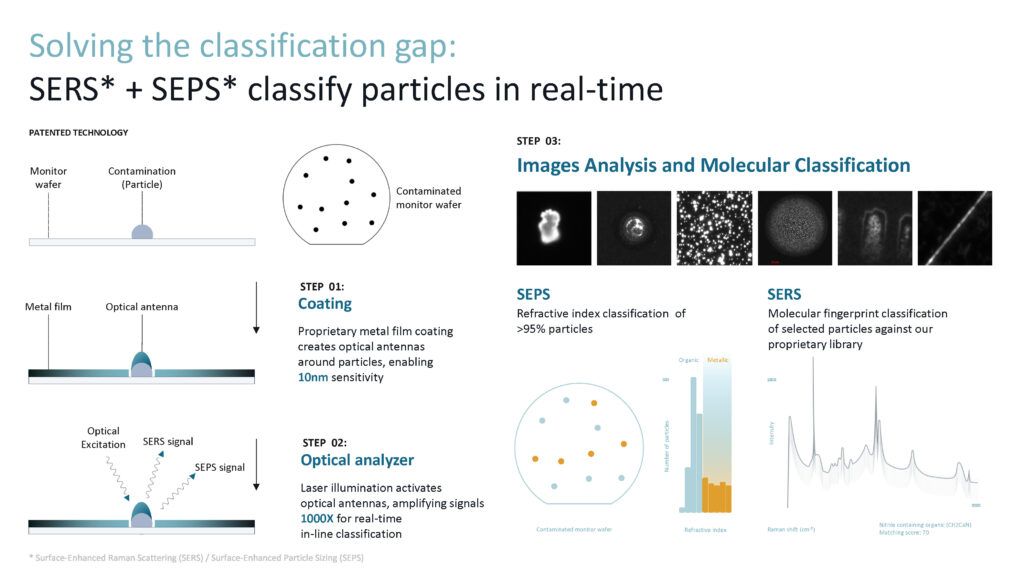
Our technology is a three-step process that starts with an unpatterned wafer. First, we apply a proprietary metal film coating to create an optical antenna for each particle. In the second step, light in our optical analyzer activates the antenna, amplifying signals for both imaging and spectroscopy. In the third step, image and spectroscopy signal analysis are used for particle classification.
Our proprietary coating and optical analyzer work together to locate and classify particle contamination through imaging, particle sizing down to 10 nm via Surface Enhanced Particle Sizing (SEPS), and molecular characterization using Surface Enhanced Raman Spectroscopy (SERS). Our process is universal, working on any flat surface with any kind of nanoparticle—hence our company name, UNISERS.
Contamination Control Systems
Discover how our technology will improve chip manufacturing yield significantly and prevent critical yield excursions.