Molecular intelligence for semiconductor contamination classification
Our technology brings to the market a unique method for molecular particle characterization, enabling customers to find contamination sources faster.
UNISERS’ technology serves the entire semiconductor ecosystem. The areas of applications can be divided into two main categories: Defect Review and Liquid Defectivity.
Defect Review
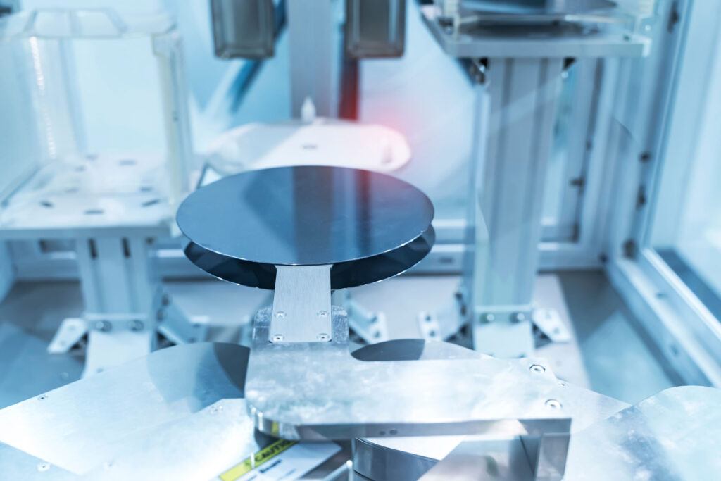
UNISERS Explorer G1 is a revolutionary system for automated defect review of 300mm wafers, bringing to the market molecular particle characterization to pinpoint contamination sources.
Liquid Defectivity
UNISERS Inspector monitors the on-wafer impacts of liquid defectivity to catch material excursions before they enter the fab.
Analysis Service
We have several generations of systems in our laboratories in Zurich to perform automated testing for our customers.
Please reach out to us to discuss how our technology can complement your sample analysis.