We're hiring! Take the next step in your career with us.

Products

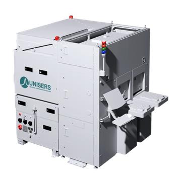
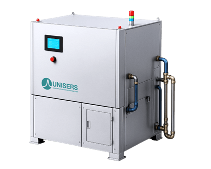
Superior Equipment for Contamination Control

At UNISERS we are helping semiconductor manufacturers to deliver a higher chip production yield.

We are developing, producing and selling equipment employing our novel and unique technology for contamination control.

Currently, we are working with our first customers to test and evaluate early versions of our commercial machines at their locations. Customers are also sending unpatterned wafers or process chemicals to our laboratory for analysis. Several future products are under development.

Please reach out to us if you would like to know more about our products and the product roadmap. We are curious to learn about your requirements.

Key Features of UNISERS Equipment

After coating in our dedicated vacuum coating process, the wafer is scanned in our dedicated optical microscope. All nanoparticles down to 8nm size are detected independent of composition of the nanoparticle and independent of the material of the wafer.

Our solution helps semiconductor manufacturers to deliver a higher chip production yield.

Our software accurately determines the size of the individual nanoparticles from the optical enhanced signals of the coating. Particle size distribution ranges from 8nm to above 100nm.

The enhanced optical images show various characteristic features that remain hidden in usual optical microscopy or even electron microscopy. Shape, appearance, agglomerations and surrounding residues allow classifications.

SERS (Surface Enhanced Raman Scattering) spectra can be recorded from selected nanoparticles at high speed. These spectra provide information about the molecular structure of the contaminants and help to trace the source.

We are building a rapidly growing data library that will help our customers to identify the source of contamination more accurately and much faster.

We have developed an additional unique technology that allows the controlled deposition of contaminants from liquids onto a wafer (or any other flat surface) in a way that mimics process conditions. This new method works not only for ultrapure water (UPW), but also other process chemicals such as IPA, H2SO4, HCl, etc.

The UNISERS Advantage

Work-at-UNISERS-Universal-Contamination-Analysis

See the Invisible

Our technology is capable of optical detection of any nanoparticles down to 8nm in size.

Work-at-UNISERS-Universal-Contamination-Analysis

Fast Results

Because of our enhanced optical methodology, you get results faster without losing quality or accuracy. 

Work-at-UNISERS-Universal-Contamination-Analysis

Greater Detail

With our technology, you can gather molecular information from individual nanoparticles (Raman signal).

Our technology works on any substrate with any nanoparticles, and customers are able to determine the accurate size distribution from all individual nanoparticles.

Our customers can easily and confidently identify the source of contamination, which results in significant cost and time savings compared to existing contamination analyzing solutions.

This results in a higher chip production yield and more profits.

Analysis Service

We have built several generations of prototypes of 300mm wafer compatible machines, which we are using in our laboratory in Zürich to perform tests for our customers.

Customers are sending us unpatterned wafers or liquid chemicals, which we then analyze.

Please reach out to us to discuss how our techniques can complement your sample analysis.

UNISERS-Analysis-Service-Universal-Contamination-Analysis